HDI · BLIND & BURIED VIAS
Models and specifications
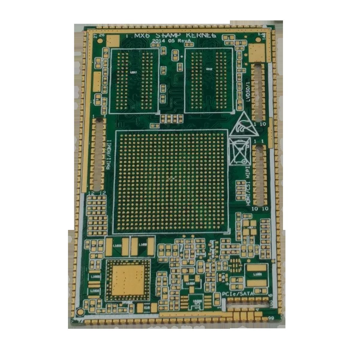
Blind & buried via board
1–3 step HDI · stacked vias / POFV · laser blind vias 0.10 mm
Get a quote for this productFull process parameters & technical features
| Capability item | Specification range |
|---|---|
| HDI build-up stages | 1 – 3 stages |
| Min. laser blind via diameter | 0.10 mm |
| Min. mechanical drill diameter | 0.15 mm |
| Min. line width / spacing | 2 / 2 mil |
| Board thickness range | 0.4 – 3.0 mm |
| Via types | Through / blind / buried / via-in-pad / stacked vias |
| Via filling methods | Resin plugging / electroplated via filling (POFV) |
| Layer-to-layer registration accuracy | ±0.05 mm |
| Laser drilling type | CO2 laser (blind-via aspect ratio ≤ 1:1) |
| Blind-via annular ring (per side) | Standard 4 mil (limit 2 mil) |
| Hole copper thickness | 25 – 50 μm (thicker on request) |
| Surface finish options | ENIG / ENEPIG / immersion silver / immersion tin / OSP |
✓Technical highlights
- Mature, reliable blind/buried via processes and stacked via structures
- Via-in-pad (POFV) frees routing in BGA areas
- Fine lines 2/2 mil for high-density breakout
- Stable laser drilling and resin plugging processes
- CO2 laser drilling with LDI direct imaging for stable 2/2 mil yield
- ENEPIG (nickel-palladium-gold) supports fine-pitch BGA and wire bonding
- Half-hole and metallized half-hole processes support modular assembly
AI accelerator cardsOptical modulesWearable devicesIoT modules5G communicationsAutomotive electronics
Ask for a quote on this board type